News

Exploring AMD Ryzen 7000: Zen 4 and AM5 architecture
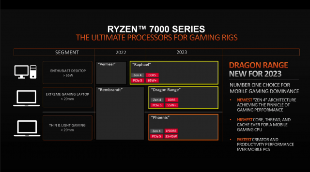
AMD has revealed the details of its Ryzen 7000 series processors on the Zen 4 architecture codenamed “Raphael”. Every now and then the results of various benchmarks that new processors become leaders in one category or another, and AMD itself mentions that the processors are the most advanced and efficient, but we will dwell on the significant results from the available information, so that everyone can make their own conclusions.
It is worth noting that AMD has not gone the way of Intel and has not introduced hybrid cores into its processors, but one innovation will appeal to some of us. The new Ryzen will now have integrated graphics; yes, it will not claim the level of discrete graphics cards, but now it will be possible to display even without a graphics card. Yes, this capability was absent in past AMD processors, except for APUs, processors that couldn’t compete in terms of processor performance with processors without graphics. A Plus Garage Doors has completely switched to such processors https://a-plus-garagedoors.ca/.
5 figures 5 and technical specifications
In order not to leave everything for later and to understand why we have 5 figures 5, let’s focus on the technical specifications.
- Processors are based on 5 nm technology from TSMC
- New AM5 socket
- Processors work only with DDR5
- PCIe 5.0 interface
- Processor Peak Frequency above 5GHz
- Bottom line: 5nm, AM5, DDR5, PCIe 5, 5GHz.
Now let’s look at the other features of the processor release.
- Up to 16 cores and 32 threads, which has remained constant since the 5000 series.
- Up to 5.7GHz in the Ryzen 9 7950x processor, while the Ryzen 9 5950x was claimed to be 4.9GHz.
- Chiplet technology, which we already know from the 3000 series. In the new generation, the chipsets with cores are made by 5 nm processor, and the I/O chipset by 6 nm.
- DDR5, which increases memory bandwidth per core by 125%.
- RDNA 2 integrated graphics, which is in the I/O chiplet with minimal power consumption.
- We’re looking at about a 29% increase in single threaded performance, about a 45% improvement in multi-threaded performance, and about a 28% increase in performance per watt.
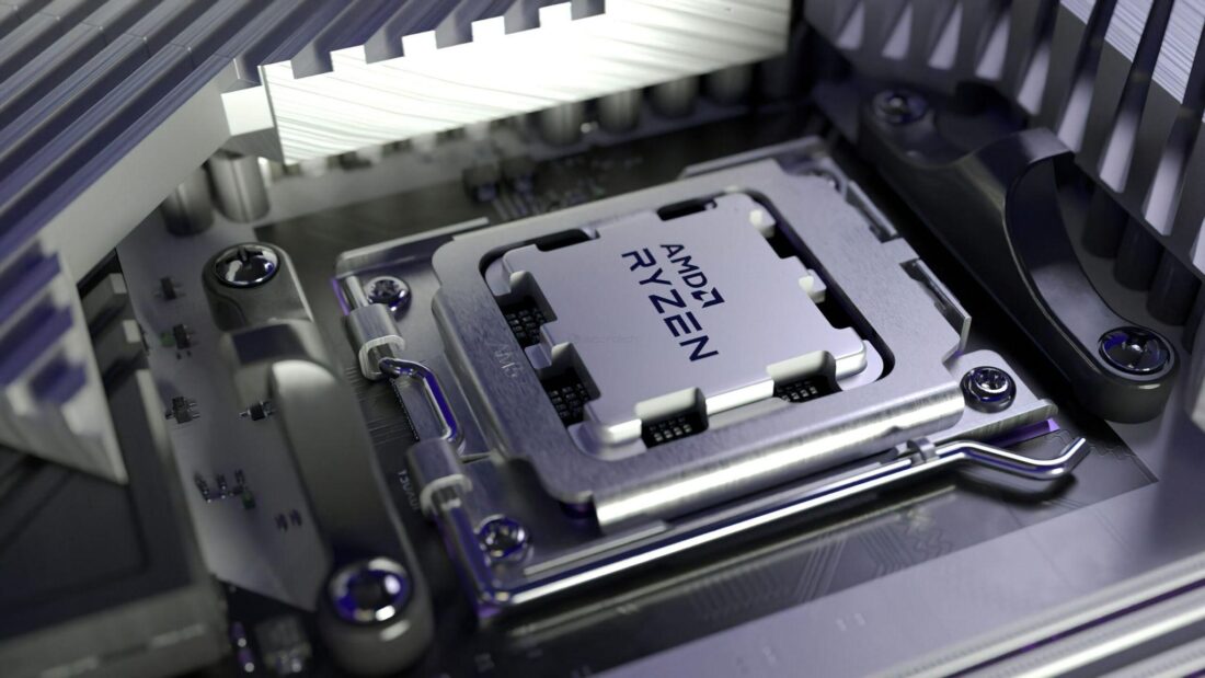
- AM5 socket LGA 1718. LGA – the socket is now similar to Intel. This is one of the forced measures, LGA technology allows in the same area to place a greater number of contacts and pads for them on the processor itself.
- 600 series chipsets: X670E Extreme, X670, B650E Extreme and B650.
- Power consumption increased to 170W TDP and up to 230W at maximum loads. Compared to last generation with 105W and 142W.
- Support for AVX-512, VNNI.
- Zen 4 processors with 3B V-Cache are announced to appear this year as well, but there is no information what kind of processors they will be.
We have seen 4 processors: Ryzen 9 7950X, Ryzen 9 7900X, Ryzen 7 7700X, and Ryzen 5 7600X. Each of them will have the number of cores and threads that we are used to seeing from previous generations of processors.
Let’s refer to the table below to see the main characteristics of the new processors.
| Model | Cores / Flows | Base / Boost Frequency (GHz) | TDP (Вт) | Cache (L2+L3) MB | Memory |
| Ryzen 9 7950X | 16 / 32 | 4.5 / 5.7 | 170 / 230 | 80 (16+64) | DDR5-5200 |
| Ryzen 9 7900X | 12 / 24 | 4.7 / 5.6 | 170 / 230 | 76 (12+64) | DDR5-5200 |
| Ryzen 7 7700X | 8 / 16 | 4.5 / 5.4 | 105 / 142 | 40 (8+32) | DDR5-5200 |
| Ryzen 5 7600X | 6 / 12 | 4.7 / 5.3 | 105 / 142 | 38 (6+32) | DDR5-5200 |
If you compare the frequency of the processors with the last generation, it has increased by 800 MHz or 16 percent. Power consumption increased by 38 percent.
Zen 4 architecture.
The Zen journey continues, so says one of AMD’s slides, which shows us the evolutionary history of the architecture, from 2017 through 2022. Of course, it’s not over yet, waiting for further developments, but at this point we can see the major changes. With each generation, the maximum frequency and IPC increased, and different architectural changes took place. With Zen and Zen+ we saw 8 mb cache per complex of 4 cores, SMT (simultaneous multithreading or multithreading technology, when one core has two threads), new boost algorithms and 14/12 nm technology.
With the advent of Zen 2 appeared chip design, full support of FP-256 instruction, increased L3 cache from 8 to 16 Mb and reduced to 7 nm technology process. It is worth to pay attention that AMD primarily focuses on the chiplet’s chipset process with cores rather than I/O chipset.
Going a bit off topic, I/O chipset still has a different techprocess, albeit much smaller than it was before. In Zen 3 AMD showed complexes of 8 cores within a single chiplet. Whereas Zen 2 had two 4-core complexes in one chipset, now one chipset = one 8-core complex, also L3 cache is up to 32 mb with the topology changed. At the same time the process technology remained at the same level. In Zen 4 the technical process was decreased and now it is 5 nm, complex of cores remained unchanged, L3 cache topology was changed once again, at the same time we left its volume. We increased L2 cache up to 1 Mb, as well as added RDNA2 graphics core. Now we can display images on the screen without any video card, only with the help of the processor.
Now let’s turn to the topology of the chip itself with 2 CCD’s (2 complexes of 6-8 cores each) + IOD (I/O chipset) which are the older 7900x and 7950x models. Everything is learned by comparison, and we will look at the new topology in relation to Zen 3 architecture. If we talk about the CCDs themselves, there are no changes in topology.
There are still 8 cores 16 threads, 32mb L3 cache for each of CCX in CCD, same as last generation we see Infinity Fabric bus, in this case number of read and write cycles remains the same as in Zen 3. Now let’s move on to the cIOD. In this block, the communication speed between Infinity Fabric and Unified Memory Controller, as well as between Infinity Fabric and IO Hub Controller remained the same.
SyncFIFO
However, one interesting SyncFIFO block appeared. In fact, AMD has already claimed patents for this technology in 2019, 2021, perhaps some time yet. The technology itself is not new, something similar was already slipped in 2005. The block itself operates the first-in-first-out (FIFO) buffer with the first clock pulse and one of the FIFO buffer read or write pointers with the first frequency, while operating another read or write pointer on the second clock pulse.
One of the serializer, fed from the output of the buffer FIFO, or deserializer, feeding data to the input of the buffer FIFO, operates with the second clock pulse. Timing pulses let the pointer operating with the second clock pulse, that it has reached a set point in its cycle. The phase of the second clock pulses is adjusted based on the relationship between the timing pulses and the lead period of the pointer operating with the first clock pulses. The pointer operating with the first clock pulse is reset to achieve the desired ratio value.
It corrects for the skew that occurs when you adjust the phase of the second clock pulses. This sounds rather complicated and is only a general description. So why is this block needed? Simply put, if in Zen 3 fclk = uclk, now it is not necessary, the block itself synchronizes the frequency at runtime according to its algorithms.
This is far from saying that the IF frequency has become second nature, but now with 6000 MHz memory frequency there is no need for fclk = 3000. Moving on to the communication between the Unified Memory Controller and the memory, there has also been a change here. Since each RAM module now has 2 channels, the data is now also sent via two channels from the memory to the Unified
Zen 4
In “Zen 4” AMD introduces AVX-512 support, aiming to improve processor performance in high performance computing and artificial intelligence tasks. According to AMD claims the implementation has been done in the most compact and energy efficient way possible, without affecting the processor’s core frequency. AVX-512 operations are performed on a 256-bit dual-filled FPU rather than a 512-bit FP mechanism.
The VNNI and Bfloat16 instruction sets have also been added, which means that “Zen 4” can handle almost all the AVX-512 client-related workloads that competing processors from Intel can currently perform.
The load/store block is the part of the core that interacts with the memory subsystem. The “Zen 4” kernel gets a 22% increased boot queue with improved resolution of data port conflicts. The reserved data transfer buffer L2 is increased by 50%. Besides that we have 3 operations per cycle, maximum 3 loads, 2 stores and 6 table (page) bypassers.
The Ryzen 7000 desktop processor’s cache hierarchy is similar to that of the Ryzen 5000 with some key differences; in addition to bandwidth/retention improvements, the dedicated L2 cache size has been doubled to 1MB. The eight CCD processor cores share a monolithic 32MB Level 3 cache with equal access to each core.
Mason
0